Utilizing Computed Tomography (CT) for Printed Circuit Board (PCB) Inspections and Reverse Engineering
3D Engineering Solutions has expertise in inspection and reverse engineering for many different applications. We combine the best available equipment and a well trained staff to deliver correct results in a rapid manner.
For PCB’s, we use the Nikon X-Tek 160kV Industrial CT Scanner which is designed to meet every need related to the inspection of PCB’s. It provides up to 160kV and 20W power, a 1µm X-ray focal spot size, and a magnification range of 2x-600x. The detector can also tilt to a max angle of 75° which provides extra flexibility in examining multi-layer boards.
Traditional Computed Tomography (CT) is well not suited to objects like PCB’s due to their high aspect ratio (width related to thickness). Typical CT scanning requires that the sample is rotated a full 360 while being exposed to X-Rays (image below). The amount of attenuation (blocking or absorption of x-rays as they pass through a material) is recorded at each projection (x-ray image) on the detector. A computer is used to reconstruct the object from the attenuated images (typically thousands of x-rays). A sample must be sufficiently penetrated by the x-rays at all angles to produce a quality data set. Due to the geometry of PCB’s having a very small thickness when compared to the width, this leads to problems in acquiring a quality CT scan. When performing a CT, the x-ray energy must remain constant during the scan. Because of this, these attenuated images captured by the detector (x-ray images) can be too saturated (washed out) when the x-rays penetrate through the thinnest parts of the board, or could be under exposed when having to penetrate through the entire length of the board.
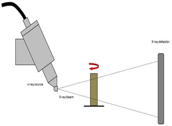
Typical CT Scanning Process
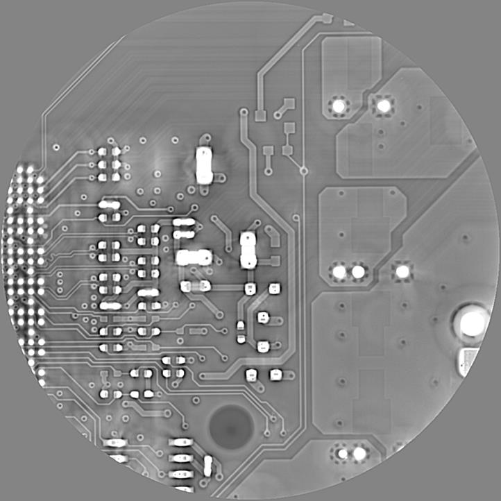
Additionally, simple X-ray inspection of multilayer boards has typically been problematic because all of the layers are included in a single image. Overlapping components can obscure others components or defects. This is because the x-rays images are an accumulation of the effective density of the entire object at once, two components positioned on separate layers will appear as one component or a blend of the two. So if traditional CT and simple x-rays are not sufficient to capture all of the critical information on PCBs, what is left?
3D Engineering Solutions employs Nikon’s proprietary X.Tract software and laminography, or Oblique Computer Tomography (CT). This allows us to produce 3D image from a region of interest on a high aspect ratio object. This is accomplished by rotating the object perpendicular to the X-ray axis as shown in image below. The aspect ratio is no longer a factor with this type of CT. With a reconstructed dataset the software allows you to scroll through 2D slices from any direction providing concise views for each layer. Vertically, the data is very good and allows precise imaging of each board layers. Horizontally, there is some added noise but not enough to interfere with our inspection and reverse engineering work.
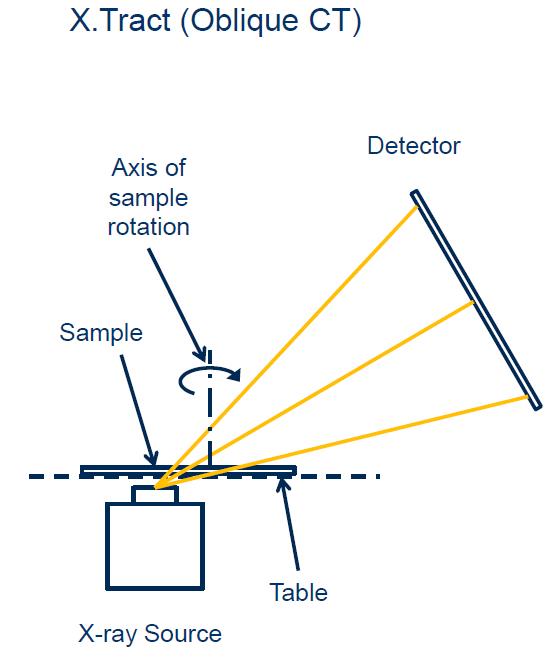
Laminography Process
REVERSE ENGINEERING
Traditionally, reverse engineering a printed circuit board (PCB) has been a destructive process. For multilayer boards, all components are removed from the surface, each layer is scanned, and an abrasive is used to remove outside layers to allow access to those underneath. With advances in X-Ray technology, boards can be mapped through non-destructive means. The number of layers in a PCB can be easily identified through laminography. Additionally, traces can be accurately mapped over the entire PCB. An entire board can be scanned and the images stitched together for each layer of the PCB.
INSPECTION
3D Engineering’s Nikon X-Tek 160kV Industrial CT Scanner also contains a variety of software for the analysis of pads and ball grid array’s (BGA’s). With the small spot sizes and large magnification achievable, defects common to soldering can be detected. Porosity is commonly found in solder, but can have profound effects on the shear strength. X-ray radiographic inspection is the best way to measure pore sizes and overall percentage. Solder joint cracking can often be spotted through a visual inspection; however, this is not always the case. The image below (red cross-hairs) shows a crack inside of the solder joint that cannot be seen visually. X-ray radiographic and CT inspections provides unmatched data for inside structure, repeatability testing, quality control, and failure roots.
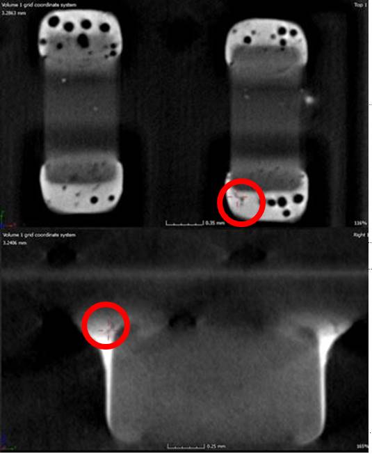
X-Ray of Crack Defect in Solder
Please contact 3D Engineering Solutions today for your x-ray and metrology needs.


Leave a Reply
Want to join the discussion?Feel free to contribute!