CT Scanning Void Detection – What to Ask for and What to Expect
Radiographic testing is a widely accepted method for finding voids and defects in materials. Makers of castings and solder connections on printed circuit boards have used radiographic testing to detect voids in 2D images and Computed Tomography (CT) in 3D images with excellent results that are well documented. As CT scanning continues to evolve and emerge as the inspection method of choice new challenges arise. Many times customers are unaware of the difference and apply old specifications on their drawings that may no longer apply. Or they do not know the full capabilities of the newer technologies or have not yet defined the specifications for their application.
Additive Manufacturing (3D Printing) is an area where this is especially true. New components are being designed that could never have existed before and new specifications for defect detection have to be applied. We often hear from customers that they want to see every possible defect in their 3D printed parts. While this is possible, they usually do not like the result of this all-encompassing request. The advanced software that is used to analyze CT scan data is able to discretely interrogate each voxel element (a voxel is a volumetric pixel – the basic unit of CT data). Turning off all of the filters to reveal every possible defect allows the software the potential to select false positives. This makes the resulting defect list show thousands of indications when in reality there are only a few or possibly none. Most false positive indications in these cases are random noise that the software can filter out with reasonable settings.
The obvious question then is: What is reasonable? The answer must be approached on a case by case basis. What is the part made out of? Is it a single or multi-material? How large is the area of interest? How thick is the part?
The trick is to have enough power available to penetrate the parts without obscuring small details like defects. As you increase the power used to create the CT data, you also increase the native or characteristic noise (that noise which is typical in the nature of x-ray generation) that may affect the results. Part density, whether there is one or multiple different materials and the overall thickness of the materials all affect this equation. You will always be able to get data from CT. However, the data may not always be clean enough to provide reliable data at the resolution needed.
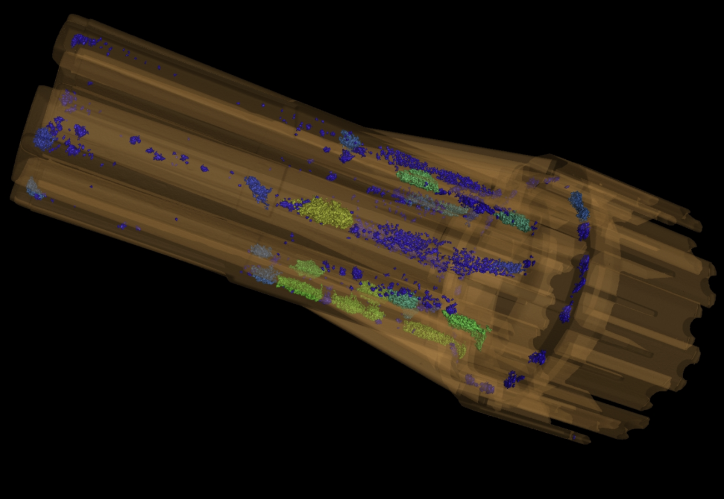
Examples of the issues include the following common examples:
- Plastic parts with metal inserts or parts made with metals of very different densities. Because the parts have relatively very different densities, the lower density material usually is either mostly blown away (made transparent in the data) by the power needed to image the higher density material or is noisy due to beam hardening artifacts and so defects are not easily resolved. If we are interested in only the higher density material, these issues go away.
- Single material parts can be difficult because of size or density. Single material parts like plastics and aluminum are easier to penetrate and show defects quite easily. However, parts made from Inconel or other high nickel content are very difficult to scan at very high resolutions. They typically need more power and lower resolution scans for accurate defect detection.
- Part size is another important factor when considering defect analysis. It is possible that even though the part material is easy to CT with great results, the overall size of the part requires a high degree of magnification to find the small size of defects that are specified in the drawings. In CT data collection, the method of magnifying is accomplished by putting a greater space between the part and the detector and a smaller space between the part and the source. To scan an object with the highest resolution its center of rotation must be as close as possible to the source. For large parts, the distance from the source may be the limiting factor for defect detection. In other words, the part may not be able to be moved close enough to the x-ray source before enough magnification is achieved due to its size.
- Total overall part thickness can also create problems even in less dense materials. Since the x-rays have to penetrate fully through the part to the detector, a sufficiently thick part can add to the noise and reduce the available resolution.
3D printed parts are becoming more common in manufacturing and bring a few new issues to add to the traditional ones in CT scanning. Typically, a void is a small pocket of air trapped inside a part. It is defined in the software as an area of lower density surrounded by higher density “material”. In the case of 3D printed parts, the lower density may be powder that has not melted. This can be very difficult to identify since the defect may only be one layer thick and only a few microns wide. These defects can look like random noise in the data and require longer scan times and larger defects for an accurate analysis.
One method of defect detection strategy is to look for indicators that are no smaller than eight voxels. Remember that a voxel is a pixel in 3D. A 2x2x2 set of voxels is usually the smallest defect we look for. Anything smaller is typically indeterminate from noise. This means to find a targeted defect size of 100 microns, a resolution of at least 50 microns is required (2x2x2 set of voxels at 50 microns per voxel).
The CT analysis software’s sub-voxel surface determination accuracy may detect smaller defects than our minimum, and depending on material properties the smallest defect detectable varies. This can be deceiving when having 8 voxels in a row (instead of a 2x2x2 set). Another parameter used to help sort for this difference is the diameter of a defect. This is defined by the smallest sphere that totally encompasses the defect. So, having a 50 micron resolution might yield a 400 micron defect diameter if those voxels were all in a row. This sounds like a large defect size. However in reality, it will have a tiny volume compared to the size of that sphere and will be very difficult to find. Since the software can show these volumes, this can be used for sorting as well. If the volume of the defect is a tiny fraction of the overall sphere volume, it can be discounted as indeterminate.
So resolution of the scan, size in voxels and compactness of the void must be taken into account when determining the minimum defect size that can be reliably detected. While most customers want to know of every void in their part, they must determine an absolute minimum that would not affect their parts design intent. If they ask to see all voids that the software can detect, then they will be generally disappointed as data noise will be detected as voids and obscure what is really happening.
If they are concerned about small voids spaced closely together in large quantities, there is a way to handle this. The software has a function that will indicate the distance from the closest void. This can be used to give an idea of the proliferation of the voids and could also be a parameter to place in the part drawing. This can also be displayed visually in the software. Even for this consideration, the same rules apply concerning the smallest size of defect and detectability mentioned above.
Your CT scanning service provider should be able to tell you the expected resolution of the scan based on the size of your part and their knowledge of their equipment. This will not be exactly known until the part is actually set up in the machine (as scanning orientation plays a part). Based on this and using the 2x2x2 voxel set rule, you can determine the smallest reliably detectable size of defect that can be seen. If you need to see defects smaller than this in a reliable manner, you will not be able to. This is at the limit of the technologies reliable detection capabilities.
While no part is perfect, understanding what can be detected reliably will yield the best results in your inspections. Contact 3D Engineering Solutions today to discuss your additive manufacturing defect detection needs.


Leave a Reply
Want to join the discussion?Feel free to contribute!